
What Equipment is Used in PCB Board Assembly Manufacturing?
Used in PCB Board Assembly Manufacturing
A printed circuit board is the brain of all electronic devices, and it’s quite an interesting thing to see how it comes together. Each stage of assembling is carefully thought-out to produce a functioning device that’s both durable and safe to use.
PCBs are made using several types of equipment and tools, some of which are specialized for specific tasks such as soldering, etching, and surface mount technology (SMT) components placement. It’s also important to maintain these machines, as a lack of care or maintenance could result in costly downtime and faulty production.
The first step in the PCB assembly process is to apply a paste layer to the board’s surface, followed by placing SMT components. Typically composed of tin, lead, and silver alloys, solder paste is a grey-coloured goo that holds the individual parts in place on a bare board. Without it, your finished product wouldn’t work!
Printed Circuit Boards (PCBs) are the backbone of modern electronic devices, serving as a platform for connecting and supporting electronic components. pcb board assembly manufacturing refers to the process of constructing a fully operational circuit board by integrating various electronic components, such as resistors, capacitors, and microchips, onto a PCB.
This assembly process is integral to the production of electronic products ranging from consumer electronics to medical devices, automotive systems, and industrial machinery. The manufacturing of PCB assemblies involves multiple steps, including design, prototyping, assembly, and testing, with high precision required at each stage to ensure optimal functionality.
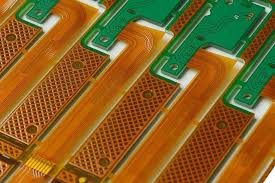
What Equipment is Used in PCB Board Assembly Manufacturing?
Once the solder paste is applied, a Pick and Place machine takes over to pick up each component and then place them on the board. This is a crucial PCB manufacturing technique that allows for high-speed and precise assembly, while also reducing human error. Depending on the type of equipment, these machines can handle up to 30,000 components per hour.
After the component placement and reflow soldering steps, it’s time to test and inspect the finished product. Various tests can be performed, including visual inspection, Automated Optical Inspection (AOI), and in-circuit testing (ICT). In-circuit testing is an especially crucial part of the process, as it checks how the individual components interact with each other and the rest of the circuit board.
There are a few different techniques used to assemble PCBs, but the most popular is called reflow soldering. Reflow ovens are specialized pieces of machinery that look like giant ovens and have different temperature zones. When a circuit board is placed inside, it’s heated and melted by the reflow solder to bond with the component leads. This method is ideal for smaller components like BGA and QFN, and it offers a high welding quality.
In contrast, wave soldering is better for larger components and can be used on FR-4 boards. In this process, a layer of flux is applied to the SMD pads and components before passing them through a wave of molten solder. This type of soldering is more efficient than reflow soldering, but it’s not suitable for all applications, such as those that require a low melting point.

Google to start restricting third-party cookies from January, completely disable them by mid-2024

After billions spent, why is polio still spreading in Pakistan and Afghanistan? – Firstpost

Can CrossFit help people with long-term health conditions? – Firstpost
About The Author
