
IC Substrate: The Foundation of Integrated Circuit Packaging
IC Substrate: The Foundation of Integrated Circuit
IC substrate—also known as chip substrate—is one of the most fundamental components in today’s electronic devices. It plays a crucial role in the fabrication of IC chips, and its structure and technology adapt to the evolving needs of modern device design and development. The continuous improvement of structure and manufacturing technology has allowed IC substrate to become the core of a precise, efficient system that supports innovative device designs and advanced features.
An IC substrate’s key functions include signal transmission, heat dissipation and electrical performance. A well-performing IC substrate can offer fast and stable signal transmission, which is vital for the performance of electronic devices. It also facilitates effective heat dissipation, preventing overheating that can damage equipment.
A common ic substrate design includes conductor layers, insulating layers and pads for connecting IC chips. The layout of these layers affects the signal transmission speed and performance, while the pad and pin design can influence IC chip performance and reliability. IC substrates also need to be lightweight and durable enough for multiple bonding methods.
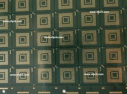
IC Substrate: The Foundation of Integrated Circuit Packaging
To improve IC substrate design and manufacturing, the industry has adopted high-density interconnection (HDI) technology, which offers higher performance by using fine lines and stacked structures. HDI substrates are also designed to support the latest IC packages, including BGA and CSP.
In addition to the need for superior design and performance, a reliable IC substrate must also meet stringent process requirements. This means achieving a high overlay accuracy and delivering high yield rates. To ensure this, manufacturers must employ advanced inspection techniques that use automated optical inspection (AOI) systems to detect voids and other defects. Advanced root-cause analysis can be applied to the AOI data and CAM outputs to deliver improved quality and yield.
The process of producing an IC substrate requires many steps, starting with patterning the surface. A patterned surface is then immersed in a copper electroplating bath to deposit a layer of copper on the patterned substrate. The coating process must be consistent to achieve uniform copper growth. A poor copper plating finish can cause a number of problems, such as uneven distribution of the metal and poor solderability.
Finally, a surface finishing step is required to make the IC substrate smooth and durable. Several types of surface finishing processes are used, depending on the type of IC package. For example, a substrate intended for a BGA IC package needs to have a high electrical performance and good thermal dissipation.
IC substrate production requires special care to address yield-critical challenges. To ensure optimal results, IC manufacturers should invest in advanced AOI technology and work closely with designers and equipment suppliers. This approach can help them improve product quality and performance and achieve better yield rates, while improving their overall competitiveness. By working together, the entire electronics ecosystem can develop long-term partnerships that lead to better quality and lower costs.

India recorded 51 ragging-related deaths in colleges from 2022 to 2024: Report – Firstpost

What are NB.1.8.1 and LF.7, the 2 new Covid-19 variants detected in India? – Firstpost

China’s Big Tech firms like TenCent, Alibaba are buying up lots of properties following real estate crash
About The Author
