
What Are the Applications of HDI PCB?
Applications of HDI PCB
The digital world is becoming more complex hour by hour whereas the hardware associated with it is getting drastically smaller. This is the reason why high-density interconnect (HDI) printed circuit boards are gaining popularity worldwide. They allow for more circuitry in a much smaller area, thus helping manufacturers create small electronic devices that are not only compact but also highly functional.
HDI PCBs are ideal for situations where space, weight and reliability are primary concerns. They offer greater flexibility in component placement and a number of benefits that make them more cost-effective than standard PCBs. For example, the use of blind and buried vias in an HDI design allows for thinner traces and reduces power consumption. In addition, the use of microvias helps to improve signal integrity.
In order to produce an hdi pcb, first the copper foil layer is laminated onto a substrate or core material such as FR-4, metal or polyimide. Then, the layers are drilled, plated and filled with various materials depending on the design requirements. Typically, the holes are made using mechanical drilling or laser technology. These holes act as interconnections between the different layers of the board.
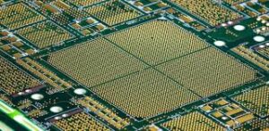
What Are the Applications of HDI PCB?
There are two main types of HDI PCB structures: build-up/sequential laminations and any-layer structure/every-layer interconnect (ELIC). The former is the most common, as it uses a sequence of sequential layers to construct the core. Each layer is then drilled, plated and filled before the next one is laid on top of it. The latter offers the freedom of any-layer interconnections and is used for more complex boards with a high pin count.
Another factor to consider is the choice of dielectric materials for an HDI board. Typically, these should be low in dielectric loss and have a low dissipation coefficient to handle the heat generated by components and traces. Moreover, they should be thin enough to minimize stress due to thermal expansion. The prepreg thickness is also important as it separates and isolates the conductive tracks.
The manufacturing process of an HDI PCB is also more demanding than other traditional PCBs. This is because it requires precise alignment and a high level of quality assurance. For instance, the etched and drilled surface should be flat, free of scratches and dents and have an excellent solderability. Additionally, the process is more sensitive to the photo tool and laminate preparation parameters, and it must be done in a cleanroom.
Other factors that contribute to the superior performance of HDI PCBs include: improved impedance control, reduced crosstalk and better ground plane and layer stackup design. Furthermore, the HDI PCBs are more resistant to electromagnetic interference (EMI) and can operate in a wider temperature range. This makes them ideal for the automotive and aerospace industries, where they can be used in harsh environments. HDI PCBs also offer improved electrical efficiencies and signal accuracy, making them ideal for high-speed and high-frequency signals. As a result, they can be used in advanced mobile phones, MP3 players and video game consoles.
Why should businesses perform web application vulnerability assessment regularly?

Russia’s cancer vaccine is ready. Here’s why it matters – Firstpost

World Cancer Day | India’s daycare cancer centres: A bold vision but can execution keep pace? – Firstpost
About The Author
